Homebrew 8-bit computer ("ZX-JAKEY")
Some time in 2018, I bought an old Zilog z80 CPU off ebay for a few quid, thinking I would build a computer. I did NOT know what I was doing, but luckily I didn't realise that at the time.
This is a brief description of the project so far, written up a few years after the last work was done on it. My memory is already a bit hazy on parts, and to my horror I can't seem to find all the circuit diagrams right now, but the below should give you an idea.
Getting started
The first thing I did was read Electronics for Dummies, which was essential reading for me! I then read Build your own Z80 computer by Steve Ciarcia, The Z80 microcomputer handbook, by William Barden, Z80 Assembly Language Programming, by Lance Leventhal, The Z80 microprocessor, by Ramesh Goankar, and finally How to Program the Z80, by Rodnay Zaks.

Once I'd figured out what most of the pins on the Z80 CPU did, the first challenge was just to get it doing something. I decided to try and keep things simple, and use either basic chips contemporary to the Z80, or modern equivalents. No cheating using microcontrollers or specialised ICs.
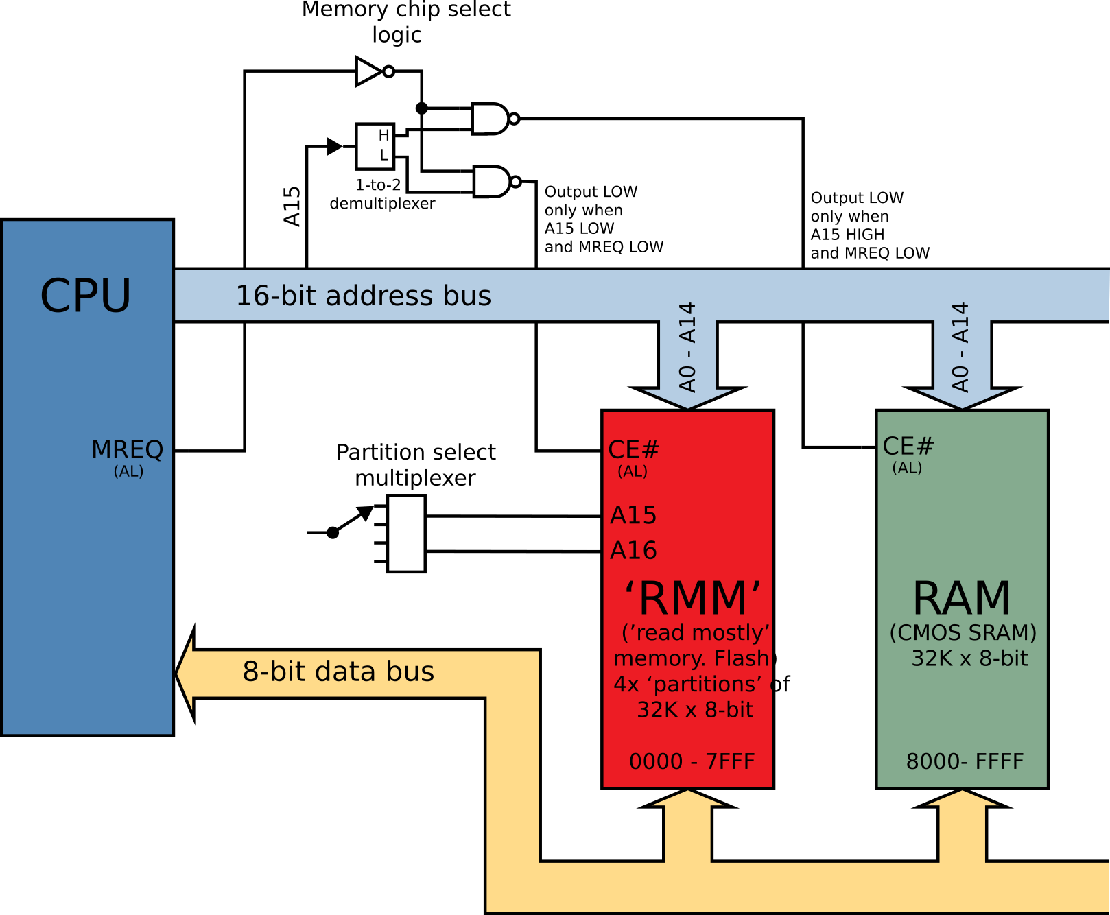
I came up with a basic setup, consisting of the Z80, a modern RAM chip, and a modern FLASH chip to serve as ROM. Because these two chips provide more memory than the Z80 can index directly, I used a physical DIP switch to select which set of addresses the CPU would be able to access. A little bit of logic meant that address line A15 would be able to select between "ROM" (Flash) and RAM, so the lower set of addresses would be ROM, and the upper would be RAM.
Flashing the flash chip
Before starting to breadboard the basic set-up, I needed some way to write data to the flash chip, that the CPU would then be able to read. Otherwise, I wouldn't know if anything was working or not.
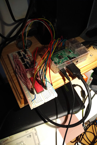
I used a Raspberry Pi to flash the chip. The datasheet for the flash chip described very clearly what the read and write sequence for chip was, giving the sequence of which pins needed to be 'high' or 'low' (+5V or 0V), and in what order.
The Pi didn't have enough useable output pins, so I had to use a few shift register ICs to be able to access all the pins.
Breadboarding the CPU and memory setup
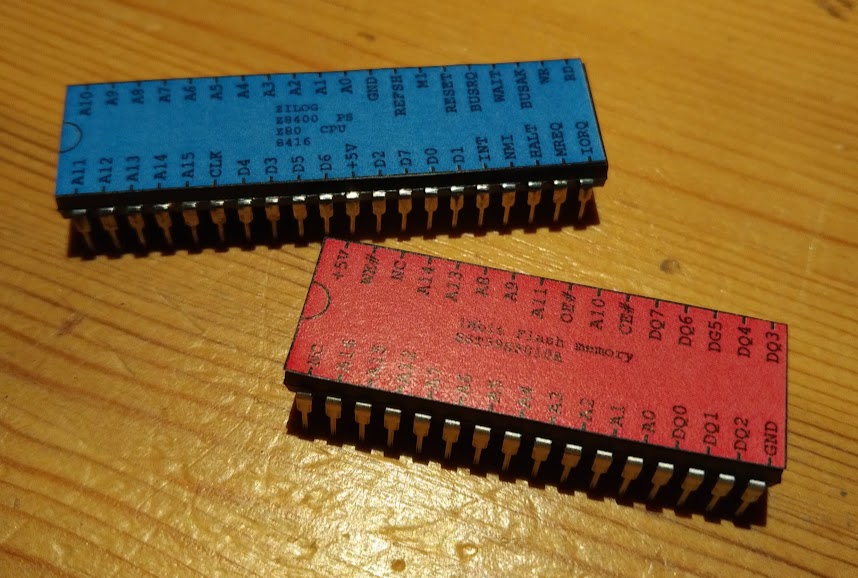
Before I began breadboarding, I took the time to design and print little stickers to put on the ICs, showing what the pins were for.
This made connecting things up much faster and less error-prone, and also looks kinda cute!
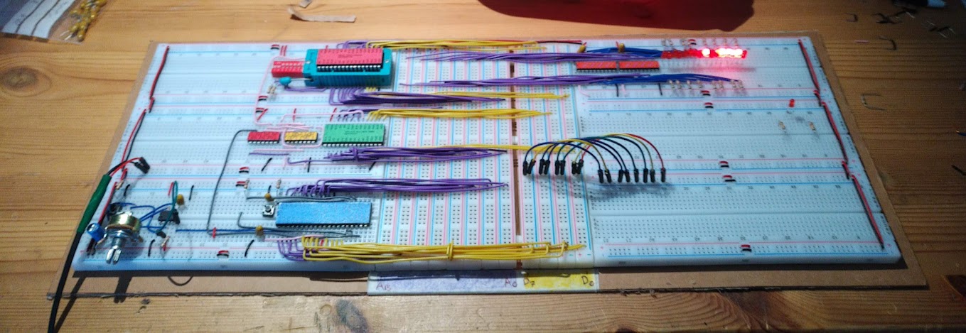
I stuck a bunch of plug-boards together on a piece of thick cardboard. Down the centre, running up and down, are the address and data buses. Off to each side are boards for other stuff. I connected all the power strips together so power and ground were always within easy reach.
For all the connections I used solid-core wire, and tried to keep things neat and tidy using different colours. Yellow are data, and purple address lines.
At the bottom left is the clock, which was just a 555 timer with a potentiometer to allow me to change the speed of it so I could watch as the red LEDs (top right) showed what was currently on the address bus. I later also added LEDs to show the data bus.
The big IC closest to the bottom is the Z80, which is connected to the address and data buses, power and ground, and a reset button (which resets address pointer).
Above that (green) is the RAM chip, with two ICs to the left controlling memory select logic. The top red IC is the flash memory, put in a socket so it could be taken off easily to flash it.
This all took several evenings of wiring to get it all connected!
A simple Z80 assembler
Up to this point I had been writing very short and simple programs directly in machine code, in order to test the basic functionality. However, this is slow and tricky, so I realised I needed an assembler - a program to convert human-readable assembly language to machine code.
I couldn't get any of the ones available online to work, so resorted to writing my own in Python. It was basic, but did the job and allowed me to write go-tos without having to keep track of memory addresses myself.
With the assembler, I could now write loops!
Printed circuit boards
I now technically had a working computer - I could get data and programs on to it by flashing the storage chip, it could run and do calculations, and I could get data off either by reading the flash chip, or by looking at the LEDs. But this isn't where I envisaged the project ending. I wanted it to be a 'proper' computer, with a keyboard and monitor, and be able to write programs on it that could then be run.
The problem was that already I had taken up a lot of the breadboard, and the connections were not great either. I clearly needed to move what I had to a more compact and permanent setup.
I toyed with the idea of using wire-wrapping to make a more permanent version of the circuit I had on breadboard, but after looking up the prices of all the stuff I needed, I decided it was too expensive. I then discovered that getting small batch printed circuit boards made is actually pretty cheap, so set about learning how to design PCBs and get them made for me.
It was a tough learning curve, but I eventually learned how to use the software Eagle to first input circuits, and then layout PCBs. Because I was pretty confident I was going to make a mistake somewhere, and because I wanted to keep the boards small and cheap, I decided to split the computer in to two boards. I would then connect the boards via edge connectors. This would also provide an easy way to add more boards down the line.
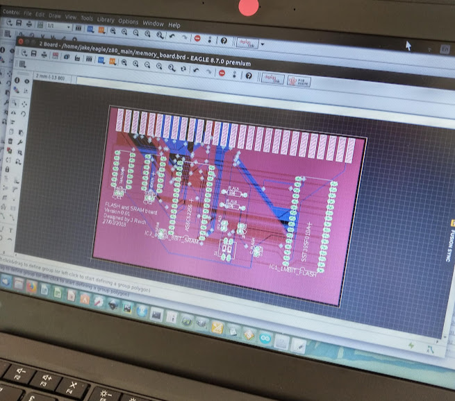
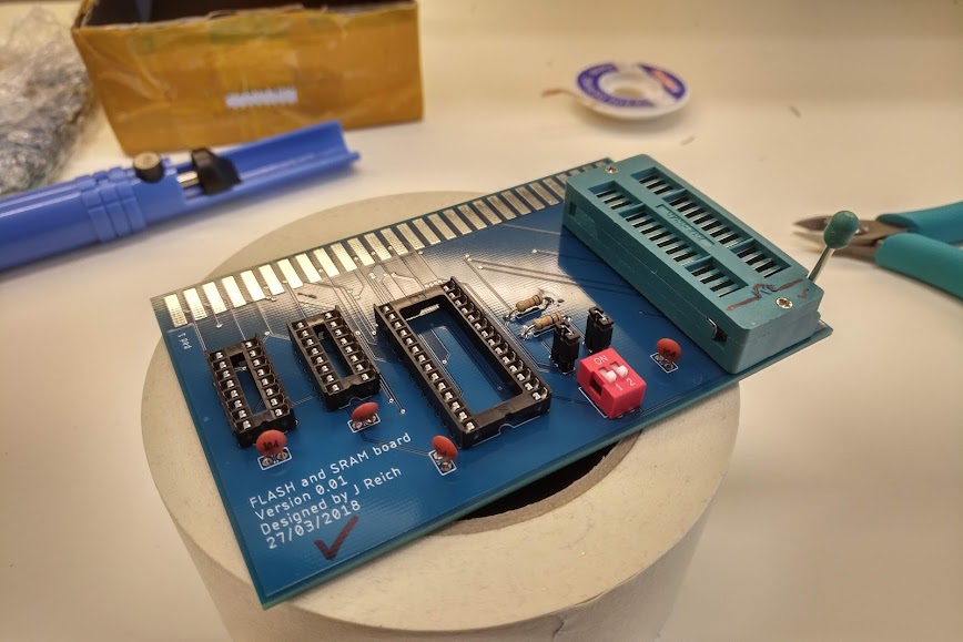
I sent off the design to PCBway, in China, and I think I paid about £40 for 5 boards. When they arrived, they certainly looked good, and I excitedly began populating one with components.
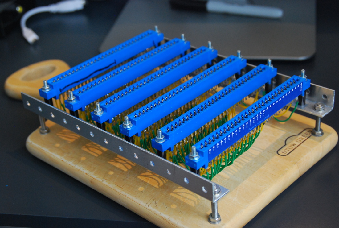
Now that I had a board with one edge made up for contacts for the address and data buses, and the other control lines, I needing a "back plane" to allow multiple boards to be connected. I had designed the edge connectors to fit in to "JAMMA" connectors, which are the standard connector used in Japanese arcade machines, and - more importantly - the cheapest I could find on ebay.
I screwed the connectors to some pre-drilled aluminium angle left over from my pen plotter project, and then carefully soldered each of the connections together. I screwed the whole thing down to the only bit of wood to hand, which was our actual bread board. I found this joke hilarious. My wife, not so much...
When testing, I discovered that I had - as predicted - made a mistake. Luckily it was an easy fix, just requiring that I drill out a connection I had made in the circuit design software, but then accidentally marked as hidden.
I had the second board already designed and ready to go, so when the memory board was delivered and looks as I expected, I had a bit more confidence to order the second board.
I got out my soldering iron and populated the board with components...
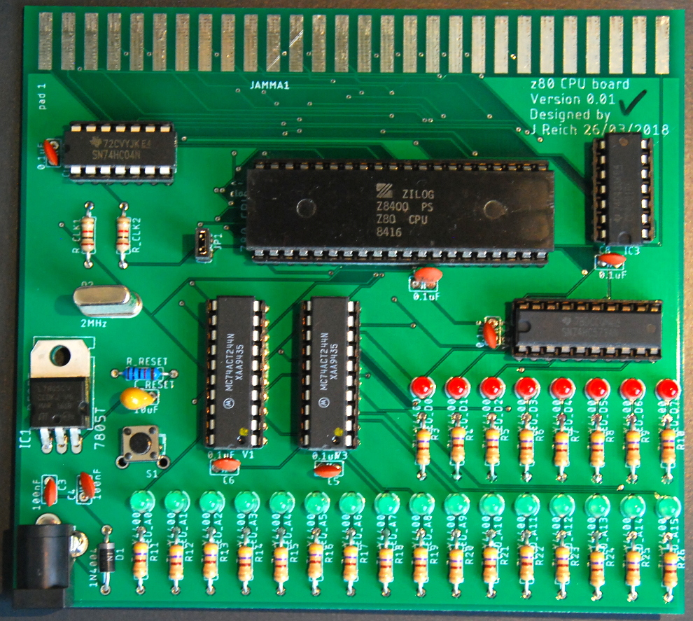
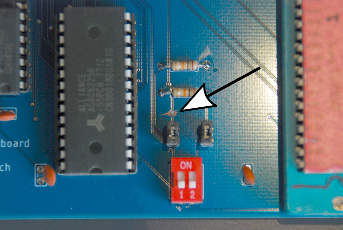
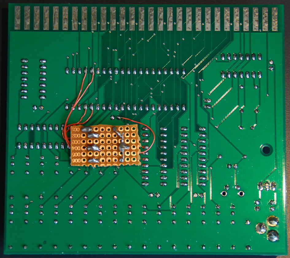
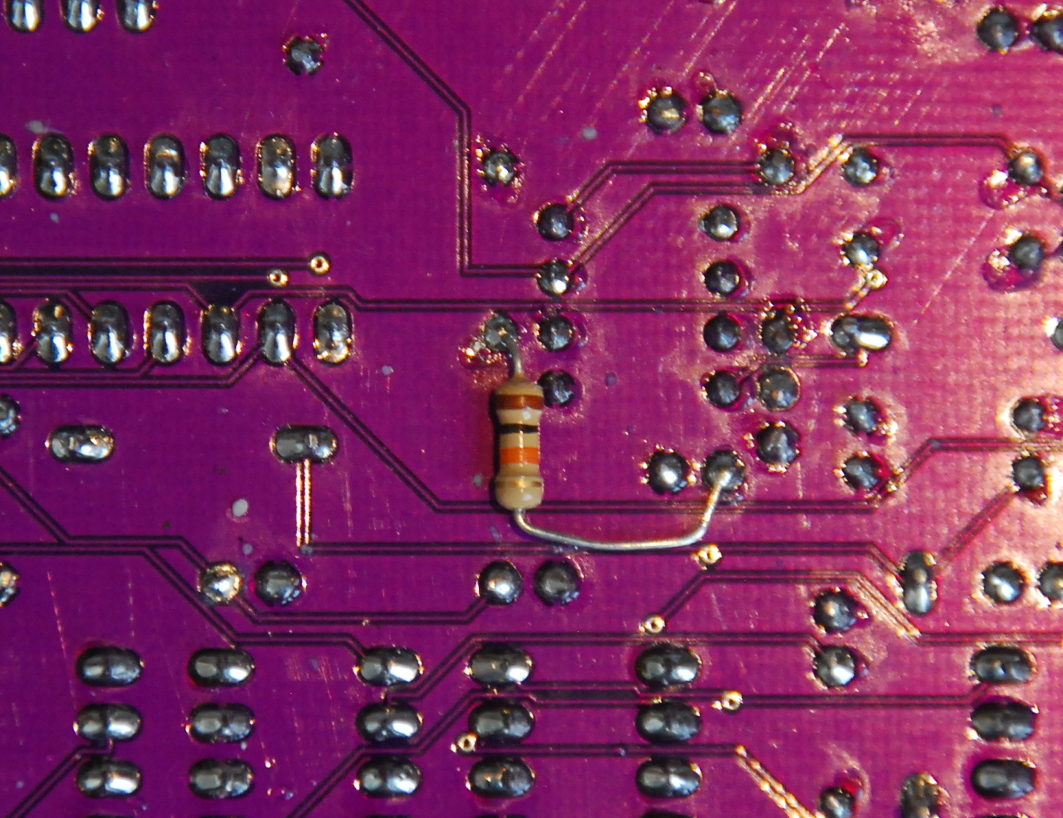
... only to discover that it didn't work. After much frustration, I eventually realised the problem, and added a fix to the back of the board. I think I had forgotten to add some pull-up (or down) resistors to some of the pins, so they would unpredictably be high or low.
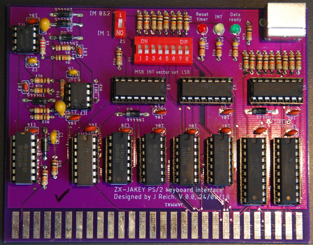
keyboard input
With the entire computer now transferred to PCBs (and functioning), I could safely dismantle the version on the breadboards to free them up for prototyping the next step, which was to make a keyboard interface.
USB is pretty complicated, and relies on the CPU (or other systems) doing things to coordinate the retrieval of data, so I opted to use the much simpler PS/2 type of keyboard. These are still commonly available, and apparently some gamers actually prefer them.
With PS/2 keyboards, when you hit a key, the keyboard circuitry just spits out a short sequence of bits in a sequence, as well as changing the voltage on some other lines to let the CPU know that there is data ready for it.
The first challenge I had was to understand what these signals look like, without the help of an oscilloscope (which I couldn't afford to buy). I managed to set up a shift register using cheap ICs to capture the data from the key board. basically all the data comes in one wire, and the shift register(s) then convert it from serial to parallel. Then I could just use LEDs to visualise the data.
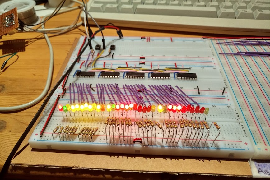
I noticed that most of the keys spat out 2 bytes, but some spat out three or four (if I remember correctly). By doing a little fudging, I could convert all the signals to one byte and still have all the keys working, except "print screen", which for some reason I can't remember sends more bytes of data.
I eventually got something working that would catch the data sent by the keyboard, and then poke the CPU to tell it something had happened. The Z80 has only some very basic interrupt abilities. Off the top of my head, I think it has one main interrupt pin (and maybe another special one). When the interrupt pin is set, the address pointer jumps to a specific address in memory (which is set using a DIP switch), which would be the start of an interrupt-handler program. In my simple case, this handler just assumes the interrupt was due to the keyboard (because there isn't anything else that could cause it), and then asks the keyboard interface to put the keyboard data on to the data bus. The CPU then saves the data in to memory. This data could then be used for whatever you want. The main operation - getting the key code generated from the keyboard in to memory - has been complete.
In order to try and keep things simple, the keyboard interface has one major limitation: if you type too fast, it doesn't work. I could go in to this, but I won't. You can always ask me for details.
video output
The next obvious thing to add is the ability of the computer to talk to a monitor, thereby enabling it to display a wider variety of data. I decided to try and design a VGA output board, as VGA is fairly simple, but still fairly common.
The VGA protocol itself is quite simple, but the main challenge for me using these old chips is speed - there is no way I could just use the CPU to generate these signals, as it's way too slow.
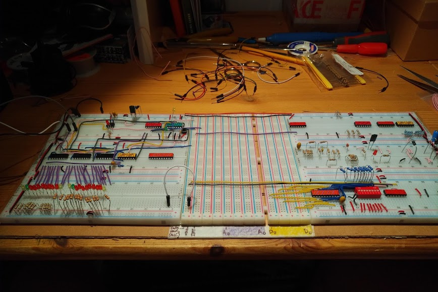
Instead, my idea is to have another RAM chip that will be accessible to the CPU via some extra circuitry. The CPU will write to this memory, and this will get read by some circuitry, and sent to a monitor. The screen buffer will be constantly read, but this reading will need to be interrupted when the CPU is writing new data to it, so the screen will go blank before it updates. I don't know much about early computers, but I think this kind of behaviour was not unheard of.
Since my daughter was born three years ago, I haven't touched this project at all, but I think I was at the stage where I just needed to write some data to the screen buffer, and see if my prototyped VGA board worked. The breadboard itself is safely tucked away in the attic, so at some point I'll get round to writing a little script to convert low-res images to the data that needs to be sent to the screen buffer.
That's all for now!
I hope you found that vaguely interesting! If you would like to get involved, especially if you have some space in which to work on the project, let me know!
Thanks!